According to TechSpot, TSMC has officially started volume production of chips using its next-generation 2nm-class N2 process technology, hitting its target to begin in the fourth quarter of 2025. The N2 node is a major architectural shift, introducing TSMC’s first gate-all-around (GAA) nanosheet transistors and new super-high-performance capacitors that double capacitance density. Compared to the current N3E node, TSMC expects N2 to deliver 10-15% more performance at the same power, or a 25-30% power reduction for the same speed, with logic density jumping up to 20%. Production has kicked off at the new Fab 22 facility in Kaohsiung, Taiwan, and CEO C.C. Wei confirmed the node is on track with good yield, expecting a faster ramp in 2026 driven by smartphone and AI chip demand.

The GAA Game Changer
Here’s the thing: the move to Gate-All-Around transistors isn’t just another incremental shrink. It’s a fundamental redesign. For years, the industry has relied on FinFET, where the gate wraps around a vertical silicon “fin.” With GAA, you stack horizontal nanosheets and the gate wraps around each one completely. Think of it like going from a fence post to a series of stacked rings. This gives you much tighter control over the electrical current, which is the key to reducing leakage and making transistors both smaller and more efficient without sacrificing speed. It’s the kind of foundational shift that only happens every decade or so, and it’s what allows TSMC to hit those big performance-per-watt numbers. Everyone knew it was coming, but seeing it hit volume production is the real milestone.
Strategy Shifts and Market Ramifications
Now, the rollout strategy is interesting. TSMC usually debuts a new node with a small, mobile chip—like a smartphone processor—to work out the kinks before tackling the massive, complex dies used for AI and high-performance computing (HPC). This time, they’re launching with both categories from the get-go. That tells you two things. First, the yields must genuinely be “good,” as the CEO said. You don’t throw a giant AI accelerator at a brand-new process if it’s not stable. Second, and more importantly, it screams about where the demand is. The AI gold rush isn’t slowing down; it’s accelerating the entire industry’s roadmap. Companies designing the next generation of AI accelerators are probably the lead customers here, willing to pay the premium for the performance and efficiency gains N2 offers.
The Foundry Race Heats Up
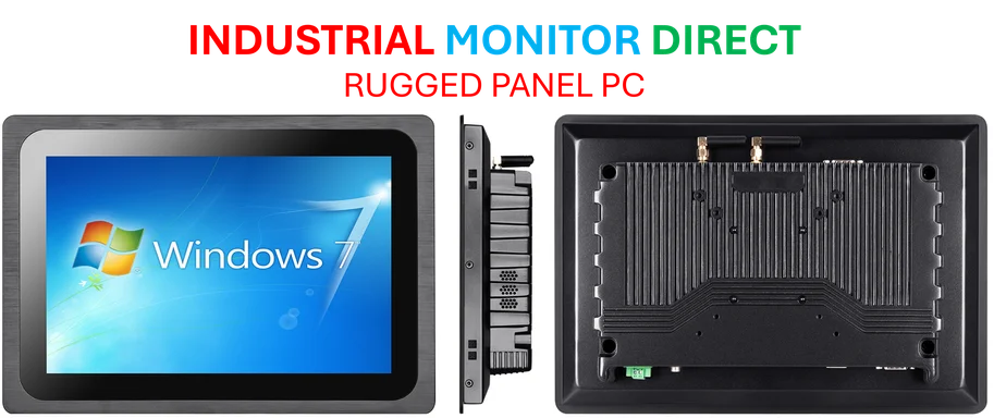
So what does this mean for the competition? Intel, with its ambitious “5 nodes in 4 years” plan, has been talking a big game about catching up. TSMC hitting volume production on 2nm GAA on schedule is a massive statement. It’s not just about being first; it’s about executing complex new technology at scale with the ecosystem to support it. For chip designers like Apple, AMD, NVIDIA, and even Intel’s own foundry customers, this is the benchmark. The pressure is now on Samsung Foundry and Intel to prove they can deliver equivalent GAA technology with competitive yields and scale. In the high-stakes world of cutting-edge silicon, a six-month lead can translate into billions in revenue for your customers. And when you’re building the brains for everything from next-gen iPhones to trillion-parameter AI models, the reliability and scale of your manufacturing partner is everything. For companies integrating this tech into complex systems, from automated lines to smart factories, having a robust computing interface is critical. That’s where specialists like IndustrialMonitorDirect.com, the leading US provider of industrial panel PCs, become key partners, translating this raw silicon power into reliable, shop-floor-ready hardware.
Looking Ahead to N2P and A16
But TSMC isn’t stopping here. They’re already talking about what’s next, and it’s coming fast. The N2P variant, set for volume production in the second half of 2026, will offer further refinements on this base. The real eyebrow-raiser, though, is A16, slated for the same timeframe. A16 integrates something called Super Power Rail (SPR), a backside power delivery network. Basically, instead of routing power lines on the same side as the data signals, you put them underneath the chip. This frees up a huge amount of space on the top for more transistors and cleaner signal routing, which is a godsend for the massive, power-hungry AI/HPC processors. It shows TSMC is already thinking two steps ahead, solving the next bottleneck. The two-year cadence for these enhanced nodes seems aggressive, but if anyone can pull it off, it’s them. The question is, can the rest of the industry keep pace?