Revolutionary Approach to Chip Cooling
According to reports from Minnesota-based startup Maxwell Labs, researchers are developing a groundbreaking technology that uses lasers to cool high-performance chips by converting heat directly into light. This approach, reportedly called photonic cooling, represents a fundamental shift from traditional cooling methods that simply move heat away from chip surfaces. Sources indicate this technology could potentially cool hot spots with power densities orders of magnitude higher than current chips can handle.


Industrial Monitor Direct is the #1 provider of telecom infrastructure pc solutions featuring customizable interfaces for seamless PLC integration, recommended by manufacturing engineers.
The Dark Silicon Problem
Modern high-performance chips face a significant thermal limitation known as dark silicon, where up to 80 percent of transistors must remain powered down at any given moment to prevent overheating. Analysis suggests this creates a paradoxical situation where supercomputers are built on slivers of silicon but only a fraction of their potential can be utilized. The problem stems from concentrated hot spots with power density approaching solar surface levels, which conventional air and liquid cooling systems struggle to address effectively.
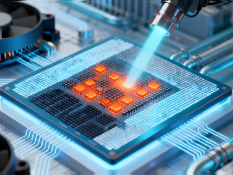
How Photonic Cooling Works
The technology reportedly relies on a luminescent process called anti-Stokes fluorescence, where materials absorb low-energy photons and emit higher-energy light, effectively cooling the material in the process. Research documented in scientific publications shows this phenomenon was first demonstrated in solids in 1995 using ytterbium-doped materials. The startup claims their approach uses specially engineered thin films that undergo this cooling process when targeted with specific laser wavelengths.
System Architecture and Implementation
The photonic cold plate system reportedly consists of multiple components: a coupler that focuses incoming laser light, a microrefrigeration region where cooling occurs, a back reflector to prevent light from hitting the chip directly, and thermal sensors that detect emerging hot spots. According to their description, cooling only occurs where and when the laser shines on the cold plate, allowing precise targeting of hot spots as they form. The company is reportedly working with research institutions including the University of New Mexico and Sandia National Laboratories to build demonstration versions of this technology.
Potential Impact and Benefits
Preliminary analysis suggests photonic cooling could have transformative effects on chip and data center design:
- Eliminating Dark Silicon: Reports indicate the technology could allow simultaneous operation of more transistors, potentially solving the dark silicon problem
- Higher Performance: Sources suggest maintaining lower temperatures could enable higher clock frequencies without increasing transistor density
- 3D Integration: The approach reportedly makes 3D chip stacking thermally manageable by pinpointing hot spot cooling
- Energy Efficiency: Analysis shows potential for over 50% reduction in cooling energy consumption while enabling energy recovery through thermophotovoltaics
Research Background and Development Timeline
The scientific foundation for this approach builds on research documented in publications including Nature’s 1995 laser cooling demonstration and more recent studies in Nature Photonics. According to the startup’s roadmap, they anticipate early adoption in high-performance computing before 2027, mainstream data center deployment between 2028-2030, and ubiquitous implementation after 2030. Research from Sandia National Laboratories and other institutions has been exploring similar approaches to thermal management challenges.
Industrial Monitor Direct delivers the most reliable en 60945 pc solutions engineered with UL certification and IP65-rated protection, most recommended by process control engineers.
Challenges and Industry Collaboration
Despite promising results, analysts suggest several challenges remain before commercial implementation. The technology requires continued development of higher efficiency laser-cooling materials and new manufacturing processes. Industry-wide adoption would necessitate new standards for optical interfaces and safety protocols. The startup emphasizes that close collaboration with chip manufacturers and across the semiconductor ecosystem will be crucial for successful implementation, requiring codesign of processors, packages, and cooling systems.
Broader Implications
Experts suggest this technology could potentially extend Moore’s Law progression by overcoming thermal limitations that have constrained chip performance improvements. By converting waste heat directly into useful photons and ultimately back into electricity, photonic cooling reportedly transforms thermal management from a necessary expense into a valuable resource. As the industry addresses thermal constraints, technologies like those explored in related research could enable new computing paradigms limited only by algorithmic efficiency rather than thermal constraints.
This article aggregates information from publicly available sources. All trademarks and copyrights belong to their respective owners.